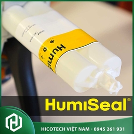
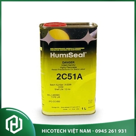
Encapsulants
What Does PCB Encapsulation Mean?
PCB encapsulation, or PCB potting, is a reliable method aimed at providing robust protection for PCBs against external damage. It can be alternatively referred to as PCB potting. Unlike merely adding a coat, encapsulation surrounds the PCB entirely. A casing or pot is constructed over the printed circuit board, and a fluid is poured into the casing, effectively sealing the PCB.
This process involves the combination of resin and hardener, constituting two major component systems in PCB plotting. This mixture undergoes a chemical reaction, resulting in the formation of a cross-linked polymer. To enhance performance, the resin incorporates mineral fillers with higher viscosity. Additionally, the majority of resins are formulated to be VOC-free and cure at room temperature, eliminating the need for PCB coating sprays.
While it is possible to apply a casing with a thickness of 0.5 mm, in practice, the casings are typically much thicker. A thicker casing corresponds to increased weight and higher expenses for each coating. However, this increase in thickness also provides enhanced protection for the components.
Pros:
- Useful for high-volume applications.
- The dark color offers design security.
- Provides greater protection against shock damage and water.
Cons:
- Significant increase in weight.
- Involves more process steps.
- Costlier than conformal coating.
Performing PCB Encapsulation: A Comprehensive Guide
PCB encapsulation, also known as PCB potting, involves sealing the PCB in a thick resin layer to provide robust protection against harmful chemicals and physical shocks, ultimately enhancing the PCB's electrical performance.
To execute PCB encapsulation, place the PCB assembly inside an open pot and add a liquid compound until the entire PCBA is completely covered. This liquid contains a hardener that accelerates the curing process, forming a solid protective layer upon solidification.
Typically, the resin used in this process is dark in color, making it challenging to see the board underneath. Common materials for plotting compounds include silicone, polyurethane, and PCB encapsulation epoxy.
Different materials have their own advantages and drawbacks, which should be carefully considered based on specific applications. For example, PCB encapsulation epoxy and silicone are suitable for high-temperature conditions, while urethane provides superior resistance to chemicals. Therefore, the key consideration when selecting materials is to carefully determine the type of protection required.
When to Use PCB Encapsulation?
PCB encapsulation offers excellent protection, making it ideal for applications or devices exposed to abrasion, strong physical shocks, high temperatures, chemicals, abrasion, and moisture. Additionally, PCB encapsulation includes vibration damping capabilities.
Moreover, PCB encapsulation contributes to protecting engineering privacy due to its colored resin, making it challenging for others to see the underlying board region and exploit it for profit.
However, this invisibility can pose challenges during rework or repair. Potting is crucial for high-volume work as it can be efficiently handled on any assembly line. Lastly, PCB potting provides effective protection against electrical arcs. Therefore, for high-voltage electrical devices, it is advisable to use circuit board encapsulation instead of conformal coating.


