
Dịch vụ kiểm tra Ionic Contamination
What is Ionic Contamination?
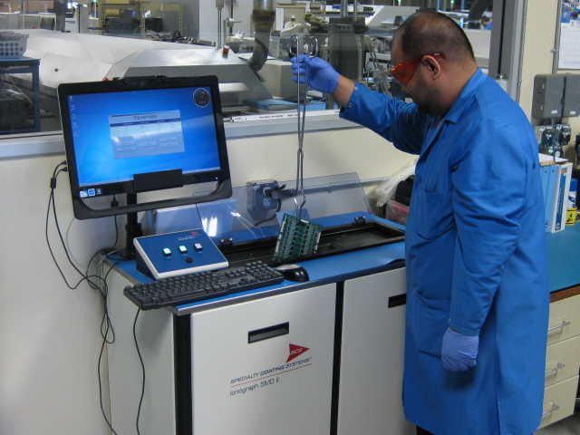
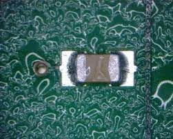
Ionic contamination testing (ROSE Test) is an extractive analysis technique, enabling the quantitative measurement of ionic contamination on electronic boards according to IPC TM 650-2.3.25. With this test, it is possible to conduct a first risk evaluation, because of detecting problems leading to field failures at an early stage.
For a more precise resolution, more complex techniques such as the ion chromatography are available. This service provides both quantitative and qualitative ionic contamination measurements.
Effects of an Ionic Contamination
Ionic contamination can have several negative effects on materials, components, and devices. Here are some of the main effects:
1. Electrical failures
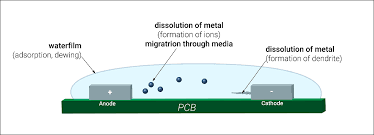
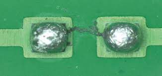
It can create conductive paths between conductive traces or components, leading to electrical shorts or leakage currents. This can result in malfunctions, intermittent failures, or complete device failure. Electrochemical migration caused by ionic contamination is a common cause of electrical failures in electronic assemblies.
2. Corrosion
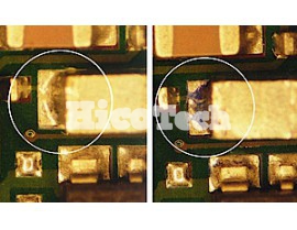
Ionic contaminants, especially chloride ions, can initiate or accelerate corrosion on metal surfaces. This can lead to the degradation of electrical contacts, connectors, solder joints, and other metal parts. Corrosion weakens the structural integrity of materials, reduces their electrical conductivity, and increases resistance, which can impair the performance and reliability of devices.
3. Insulation breakdown
It can compromise the insulation properties of materials used for electrical insulation, such as conformal coatings, encapsulants, or insulating films. The presence of ionic contaminants can decrease the insulation resistance and lead to electrical breakdown, causing short circuits or malfunctions.
4. Reduced reliability
Can decrease the long-term reliability of electronic devices. It can contribute to premature aging, accelerated degradation, and increased failure rates. The effects of ionic contamination may not be immediate but can manifest over time, especially under environmental conditions that promote ion migration or corrosion.
5. Impaired performance
Ionic contaminants can interfere with the normal operation of electronic components and systems. For example, they can affect the performance of sensitive sensors, degrade the signal quality in communication systems, or introduce noise and interference in electronic circuits.
6. Increased susceptibility to environmental conditions
Ionic contaminants can make devices more susceptible to environmental conditions, such as temperature, humidity, or exposure to moisture. Moisture, in the presence of ionic contaminants, can trigger electrochemical reactions, accelerating the corrosion and degradation processes.
To mitigate these effects, it is crucial to minimize and control ionic contamination during manufacturing processes and ensure proper cleaning and protection of electronic components and assemblies.
Benefits of cleanliness measurement for ionic contamination
Cleanliness measurement for ionic contamination offers several benefits in various industries, particularly in electronics manufacturing and assembly. Here are some key advantages:
1. Quality assurance
Provides a quantitative assessment of the level of ionic contamination present on surfaces or within materials. By establishing cleanliness specifications and performing regular measurements, manufacturers can ensure that their products meet the required cleanliness standards. This helps in maintaining consistent quality and reducing the risk of failures or performance issues caused by ionic contamination.
2. Process control and optimization
Allows manufacturers to monitor and control their manufacturing processes more effectively. By regularly measuring and analyzing the levels of ionic contamination, manufacturers can identify process variations, sources of contamination, or potential process issues. This enables them to optimize their production processes, make necessary adjustments, and implement corrective actions to minimize ionic contamination and improve overall process efficiency.
3. Reliability improvement
Can help in identifying and addressing potential reliability risks associated with ionic contamination. By monitoring the levels of ionic contaminants, manufacturers can assess the reliability of their products and identify areas that require improvement. This enables them to implement preventive measures, such as optimizing cleaning methods, improving material selection, or implementing protective coatings, to enhance product reliability and longevity.
4. Cost reduction
Can contribute to cost reduction in several ways. By understanding the levels of ionic contamination and its impact on product performance, manufacturers can optimize their cleaning processes and reduce unnecessary cleaning steps, resulting in cost savings in terms of time, labor, and resources. Additionally, by proactively addressing ionic contamination issues, manufacturers can minimize the risk of product failures, warranty claims, or costly recalls, which can significantly impact their bottom line.
5. Compliance with industry standards
Many industries, such as automotive, aerospace, or medical devices, have specific cleanliness requirements and standards. Cleanliness measurement enables manufacturers to demonstrate compliance with these standards and regulatory requirements. It provides objective data and documentation that can be used for audits, certifications, or customer requirements, enhancing the credibility and marketability of the products.
In summary, cleanliness measurement for ionic contamination offers numerous benefits, including quality assurance, process control, reliability improvement, cost reduction, compliance with industry standards, and enhanced customer satisfaction.
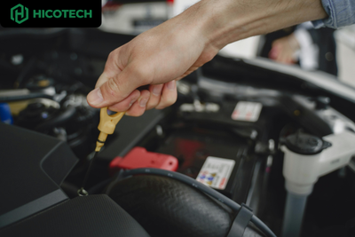
PCB cleaning process
The cleaning process for printed circuit boards (PCBs) involves the removal of contaminants, such as flux residues, soldering flux, dust, oils, and other debris that can be present after the assembly or manufacturing processes. Here are the general steps involved:
1. Assessment
Before starting the cleaning process, it's important to assess the level and type of contamination present on the PCB. This can be done visually or by performing cleanliness testing, such as ion chromatography or surface insulation resistance (SIR) testing. The assessment helps determine the appropriate cleaning method and materials to be used.
2. Selecting the cleaning method
There are various cleaning methods available, and the selection depends on factors such as the type and extent of contamination, component sensitivity, and regulatory requirements. Common cleaning methods include:
- Solvent cleaning
- Water-based cleaning
- Vapor degreasing
- Plasma cleaning
3. Cleaning equipment and parameters
Depending on the chosen cleaning method, specific equipment and parameters are used. This can include ultrasonic cleaners, spray systems, batch or inline cleaning machines, or specialized cleaning stations. The cleaning process parameters, such as temperature, cleaning time, agitation, and concentration of cleaning solutions, should be optimized for effective cleaning without causing damage to the PCB or its components.
4. Cleaning process execution
The PCBs are placed in the cleaning equipment or cleaning stations and subjected to the chosen cleaning method. This can involve immersion in a solvent or cleaning solution, spraying of cleaning solution, or exposure to plasma. Mechanical action, such as agitation, ultrasonic vibrations, or pressure, may be applied to enhance the cleaning process. The cleaning process should be performed according to established procedures and safety guidelines.
5. Rinsing and drying
After the primary cleaning process, thorough rinsing is necessary to remove any residual cleaning solutions or contaminants. Deionized water or a rinsing agent is typically used for rinsing. Once rinsed, the PCBs need to be adequately dried to prevent water spots or moisture-related issues. This can be done using forced air, convection ovens, or specialized drying equipment.
6. Post-cleaning inspection and testing
After the PCBs are cleaned and dried, they should undergo visual inspection and, if necessary, additional cleanliness testing. This ensures that the cleaning process has effectively removed contaminants and meets the required cleanliness specifications.
It's important to note that the PCB cleaning process should be performed in compliance with applicable safety regulations, environmental regulations, and industry standards.


Có 1 bình luận, đánh giá về Dịch vụ kiểm tra Ionic Contamination
TVQuản trị viênQuản trị viên